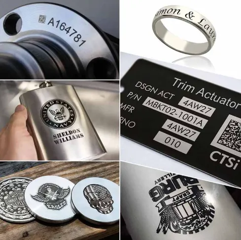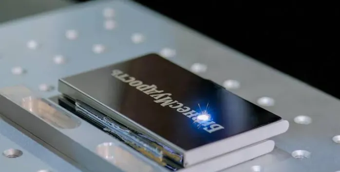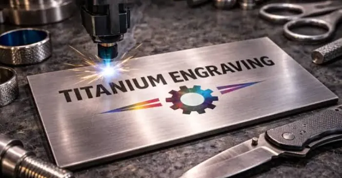
Semiconductor Laser Marking Solution
JQ Laser provides advanced semiconductor laser marking solutions for IC chips, semiconductor components and precision electronics.High precision UV laser technology creates permanent identification marks with minimal thermal impact.
Request Semiconductor Laser TestTable of Contents
Professional Semiconductor Laser Marking Solution
Semiconductor products require extremely accurate identification because of their small size, complex structure and strict quality requirements.
During semiconductor manufacturing, laser marking is used for:
- Product identification
- Batch tracking
- Quality inspection
- Anti-counterfeiting
- Production management
Compared with traditional printing methods, laser marking provides permanent, high-resolution and non-contact processing.
UV laser marking technology has become a preferred solution for semiconductor manufacturers because it minimizes thermal damage while maintaining excellent marking quality.
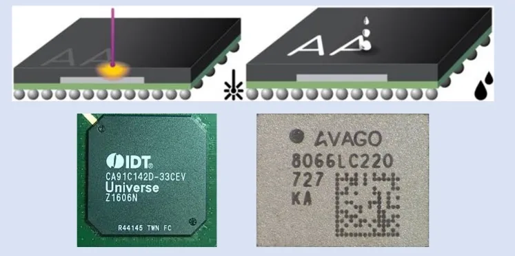
Advantages Of Semiconductor Laser Marking
Ultra High Precision
Creates micro characters, logos and identification codes.
Low Thermal Damage
Protects sensitive semiconductor structures.
Permanent Identification
Marks remain readable throughout product life.
Clean Processing
No ink, labels or chemical materials required.
Semiconductor Materials Suitable For Laser Marking
| Material | Characteristics | Applications |
|---|---|---|
| Silicon Semiconductor | Common semiconductor substrate | IC chips, wafers |
| IC Package Material | Plastic or ceramic packaging | Integrated circuits |
| Ceramic Semiconductor | High temperature resistance | Power electronics |
| Metal Semiconductor Housing | Protective structures | Electronic modules |
Why UV Laser Is Ideal For Semiconductor Marking
Semiconductor components are extremely sensitive to heat and mechanical stress.UV laser marking uses shorter wavelength technology to achieve precise material interaction with minimal thermal influence.
| Feature | Benefit |
|---|---|
| Cold Processing | Reduces component damage risk |
| Fine Beam Quality | Supports micro marking |
| High Contrast | Improves code readability |
| Non-Contact Processing | Avoids mechanical damage |
IC Chip Laser Marking Applications
IC chips require permanent identification for manufacturing control and quality management.
Laser marking can create:
- IC Model Numbers
- Manufacturer Logos
- Batch Numbers
- Serial Numbers
- Traceability Codes
High-resolution laser marking helps semiconductor manufacturers achieve accurate product tracking throughout the supply chain.
Wafer Laser Marking Solution
Wafer manufacturing requires extremely precise marking technology.Laser systems can create microscopic identification marks without affecting wafer performance.
Common Applications
- Wafer identification
- Lot tracking
- Process management
- Quality inspection
UV laser marking provides the accuracy required for advanced semiconductor manufacturing.
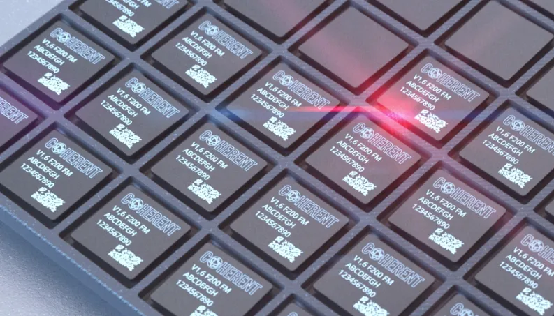
Semiconductor Laser Marking For Traceability System
Modern semiconductor manufacturing requires complete product lifecycle management.Every semiconductor component needs accurate identification information from production to final application.
Laser marking provides permanent traceability solutions by directly marking information on semiconductor products.
Common Semiconductor Marking Information
- Product Model Number
- Lot Number
- Serial Number
- QR Code
- Data Matrix Code
- Manufacturer Logo
- Production Date
These permanent marks allow manufacturers to improve quality control, production tracking and after-sales management.
Semiconductor Laser Marking Applications
| Industry | Products | Laser Marking Requirements |
|---|---|---|
| Semiconductor Manufacturing | IC chips, wafers, semiconductor devices | Micro marking, batch tracking |
| Automotive Electronics | Control chips, electronic modules | Permanent identification |
| Consumer Electronics | Smart devices, electronic components | Small characters, logos |
| Medical Electronics | Precision electronic devices | Strict traceability |
Laser Parameter Optimization For Semiconductor Marking
Semiconductor components require precise laser parameter control.Incorrect settings may affect marking quality or damage sensitive surfaces.
| Parameter | Effect On Marking |
|---|---|
| Laser Power | Controls marking intensity and contrast. |
| Pulse Frequency | Influences surface interaction. |
| Scanning Speed | Balances production efficiency and quality. |
| Focus Accuracy | Determines micro marking precision. |
Professional Experience In Semiconductor Laser Processing
Semiconductor laser marking is different from ordinary product engraving. Due to extremely small component sizes, professional experience is required to select the correct laser technology and processing parameters.
Engineers normally evaluate:
- Semiconductor material characteristics
- Component size
- Surface coating
- Required marking resolution
- Production speed
For advanced semiconductor applications, UV laser marking is often selected because of its excellent precision and minimal thermal effect.
Before production, sample testing is recommended to verify:
- Marking contrast
- Code readability
- Surface quality
- Production stability
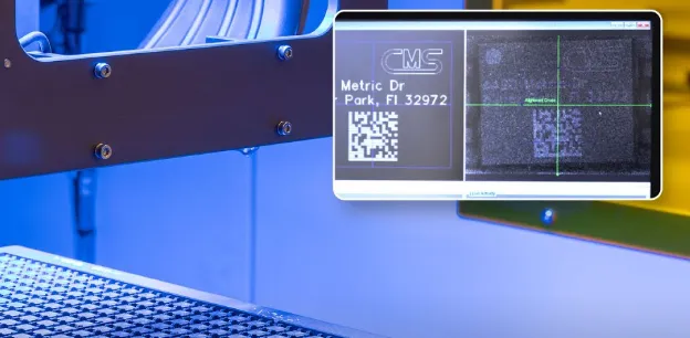
Semiconductor Laser Marking Case Study
IC Chip Micro Marking Project
A semiconductor manufacturer required high-resolution marking for IC components.The previous printing method could not achieve sufficient durability and precision.
Challenges:
- Very small marking area
- High readability requirements
- Sensitive electronic components
Laser Solution:
- UV laser marking system
- Fine beam processing
- Customized marking parameters
Results:
- Clear micro characters achieved
- Permanent identification improved
- Production tracking efficiency increased
UV Laser vs Fiber Laser For Semiconductor Marking
| Comparison | UV Laser | Fiber Laser |
|---|---|---|
| Precision | ★★★★★ | ★★★★ |
| Heat Effect | Very Low | Higher |
| Micro Marking | Excellent | Good |
| Semiconductor Application | Recommended | Limited |
Frequently Asked Questions About Semiconductor Laser Marking
What is semiconductor laser marking?
Semiconductor laser marking uses laser technology to create permanent identification marks on IC chips and semiconductor components.
What laser is best for semiconductor marking?
UV laser marking machines are widely used because they provide high precision and low thermal impact.
Can lasers mark IC chips?
Yes. Laser systems can mark IC chips, semiconductor packages and electronic components.
Can laser marking create micro characters?
Yes. High precision UV lasers can create very small characters and codes.
Does semiconductor laser marking damage components?
With proper parameters, laser marking provides controlled processing without affecting component performance.
Why use laser marking instead of printing?
Laser marking provides permanent, clean and maintenance-free identification.
Recommended Laser Machine For Semiconductor Marking
UV Laser Marking Machine ⭐⭐⭐⭐⭐
Recommended for:
- IC Chips
- Semiconductor Components
- Micro QR Codes
- Precision Electronics
Need A Semiconductor Laser Marking Solution?
Send your semiconductor samples to JQ Laser.Our engineers will evaluate your material and recommend the best UV laser marking solution for precision electronic manufacturing.
Get Free Laser Test